
Talk:Open drain
| This redirect does not require a rating on Wikipedia's content assessment scale. It is of interest to the following WikiProjects: | |||||||||||
| |||||||||||

|
This article links to one or more target anchors that no longer exist.
Please help fix the broken anchors. You can remove this template after fixing the problems. | Reporting errors |
Logical AND versus OR controversy[edit]
Shouldn't "LOGICAL AND" be changed to "LOGICAL OR"? I fixed it but let me know why it was AND -jheiv
- dlotts says: I see the source that might be creating confusion:
- http://www.acroname.com/robotics/info/concepts/opn_clct.html
- It's under the section: "Wired-OR circuits".
- If you look at the final expression, I think the line over the expression means "active low", or low voltage is 1. (Not exactly - if you're talking about pins on a chip, yes, the overbar means active low. In this case, the overbar means 'not'. Mystic Pixel) Invert it, makes it active high:
- NOT ( (A AND B) OR (C AND D) )
- and apply Demorgan's, you get a wired AND:
- NOT (A AND B) AND NOT (C AND D)
- The gates he is interfaceing are NAND gates, and that fits:
- (A NAND B) AND (C NAND D)
- So this source says AND even though it labels it OR. (No - he uses NANDs because it's active low. Mystic Pixel) Well, maybe we need a better source! Here is one:
- http://www.hardwaresecrets.com/printpage/237/10 (Note that one of the gates he's using here is a AND and the other is a NAND. That changes things. Mystic Pixel)
- The other problem seems to be with the word "active". See the Description here: http://focus.ti.com/docs/prod/folders/print/sn74hc03.html
- "They may be connected to other open-drain outputs to implement active-low wired-OR or active-high wired-AND functions."
- Hmmm. Somebody else pick it up from here. PLEASE show us your source on this page, no more "because this is correct". If no one can verify it, then well-meaning people will keep "fixing" it. Dlotts 04:06, 20 September 2006 (UTC)
- A large part of the problem is the mis-application of "logic 1". Logic 1 may be 5V, 12V, 0V, 18V, 3.7V -- the voltage doesn't matter. By saying "logic 1", we just mean "the state that represents the presence of a bit." (That hardwaresecrets page claims '1' means '5V', which is only true in an active-high TTL logic environment.)
- Now. About the word "active". "Active low" means that the low voltage state represents Logic 1, while the normal "Active high" method means that the higher of the two voltages represents Logic 1. To be frank, it doesn't mean that much -- it's just a difference in how you interpret the voltage levels.
- With that in mind, it's easier to talk about circuits in terms of "enabled" and "disabled" (this is really what '1' and '0' meant, before people started thinking '1' means 'higher voltage' and '0' means 'lower voltage'.) If you think of things this way, 'active-low' circuits are easier to handle, because the only difference is that the 'enabled' state is represented by the lower voltage instead of the higher one.
- This brings us to the central point of open-drain (and open-collector) devices. In normal devices, the output is connected to the associated voltage in both the enabled and disabled states. When the output is enabled, it is driven by the +Vcc, and when disabled, it's grounded (switch those for active-low!) However, in OD/OC devices, when the output is disabled, it is not driven by a voltage source or connected to ground! Instead, it presents a high impedance to connected circuitry -- it behaves like it is disconnected, or "open".
- If you think about things in these terms, a NAND gate can be thought of as a device that converts active-high to active-low. When both inputs are enabled/higher-voltage, the output is enabled/lower-voltage. Otherwise, the output is disabled (in an open-collector device, this means 'open'.) Make sense? (This might get confusing, because when you're doing a truth table, the output is said to be '1' for the inputs {0,0}, {0,1}, and {1,0}. This indicates the 'higher-voltage' state, which is 'enabled' for active-high logic, but 'disabled' if you're thinking active-low.)
- This is why we're using NAND gates to drive the bus, instead of AND gates (and, I think, this is why many busses use an active-low type standard.) Let's do an example.
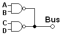
- I build this circuit with regular (not open-drain) devices. For most of the possible input conditions, both NAND gates output higher-voltage ('1', but the bus is active-low, so it's really 'disabled' in those terms.) Since these are regular devices, the output pins are connected to the higher-voltage supply, +Vcc. Now, if A and B both go to 1 (note that the input circuitry is active-high!), then the output of the first NAND goes to '0' -- (but it's active-low, so it's like the output is being 'enabled'). In order to do this, the top NAND connects the output pin to Ground. Now, since the lower gate is still connecting the output to +Vcc, the bus is connected to both ground and Vcc at the same time! The state of the bus is unpredictable at best (worst case, you've shorted your power supply!) Open-drain/Open-collector devices allow us to avoid this.


- Now, I rebuild the circuit with open-drain logic gates (note the *), and a pull-up resistor. When the gates are outputting '1', they are 'disabled' (active-low!) and thus, they are 'open' as explained above. As long as nothing is drawing current from the bus, there is no voltage drop across the resistor, and the bus voltage is +Vcc (5V in this case.) The important point is that the gates themselves are not holding the bus at +Vcc. That is being done by the resistor. If I turn on A and B, the first gate 'enables' and goes low, so it is connected to ground. Now, since the bus is shorted to ground, there is 0V on it (all the voltage from the supply goes away, because the current flow creates a voltage drop across the resistor.) This works with open-drain gates because the second gate doesn't try to drive the bus high!

- This is (one of) the benefit(s) of open-collector devices. They act as a wired OR in active low logic (using NAND gates, as above.) I just realized the source of the confusion - if you're looking at them from the viewpoint of active high logic, it behaves like a wired AND, since the bus will be '1' only when all the outputs are '1'. While this isn't wrong per se, thinking of it in those terms leads to confusion, because what's really happening is that the bus is being driven low when at least one of the gates connects it to ground.
- The article page itself is really confusing, but I can't fix it now. I hope this explanation clears things up. None of my textbooks have a good reference on this, it was something one of my professors explained a few years ago. Here are some other pages I found -- An open-collector BJT behaves the same as an open-drain FET, so the explanations more or less apply to both.
- http://kitsrus.com/zip/opencol.txt
- "As there is no pull-up resistor internal to the device an unconnected O/C output will give indeterminate voltage levels if viewed with a CRO or meter. O/C outputs can be connected together to provide greater current sinking ability or as a current driven OR gate."
- "[O]pen collector output is simply where a transistor either presents a current path to ground, or not."
- This goes back to what I was saying about enabled/disabled above.
- http://kitsrus.com/zip/opencol.txt
- http://www.mcc-us.com/Open-collectorFAQ.htm
- "Open-collector/open-drain devices sink (flow) current in their low voltage active (logic 0) state, or are high impedance (no current flows) in their high voltage non-active (logic 1) state. These devices usually operate with an external pull-up resistor that holds the signal line high until a device on the wire sinks enough current to pull the line low. Many devices can be attached to the signal wire. If all devices attached to the wire are in their non-active state, the pull-up will hold the wire at a high voltage. If one or more devices are in the active state, the signal wire voltage will be low."
- http://www.mcc-us.com/Open-collectorFAQ.htm
- I hope this helps. If you do find it useful, please feel free to re-work it into the article page (for Open drain or Open collector, since they are very similar.) Mystic Pixel 06:03, 21 September 2006 (UTC)
::::The circuit shown is actually a NOR gate, if we use logical "1"=High. Think about it. If the signal to any of the FET's is high (logical "1"), the output is low (logical "0"). Pure NOR. You must edit the page. —Preceding unsigned comment added by 134.134.136.4 (talk) 01:36, 7 December 2007 (UTC)
[edit] Definition too restrictive[edit]
There's no reason to categorize the open-collector or open-drain as an output in only digital design. I've added a plug to that hole in the two articles, but I don't know how to change the categorization or the description immediately following the subject. Python2k (talk) 16:52, 19 April 2008 (UTC)
combine with open collector?[edit]
This could be combined with open-collector and then highlight the difference as a section. This source does a good job of that. Find open-drain towards the end:
http://www.acroname.com/robotics/info/concepts/opn_clct.html
what about p channel open drain versus n channel open drain[edit]
Both are available in certain microcontrollers and it would be useful to be able to see the difference in this article ZedZzizz (talk) 05:32, 18 June 2008 (UTC)
Transistor vs MOSFET[edit]
Near the beginning of this article is a sentence that states “The word "drain" in the term "Open-drain" refers to the drain terminal of a transistor.” This is a misleading statement as a transistor does not have a “drain.” Instead the sentence should associate “open-drain” with MOSFET types devices which do have a terminal called drain. Armstrong1113149 (talk) 02:20, 13 March 2009 (UTC)
MOSFET stand for metal–oxide–semiconductor field-effect transistor 68.9.64.51 (talk) 00:34, 6 August 2009 (UTC)